Board Schematic and Pinout
The board uses two STM32F407VET6 MCUs. Both devices use the same part and pin assignment, so a normal custom firmware project can use the same pin configuration on either MCU. Only the board interface numbers are different.
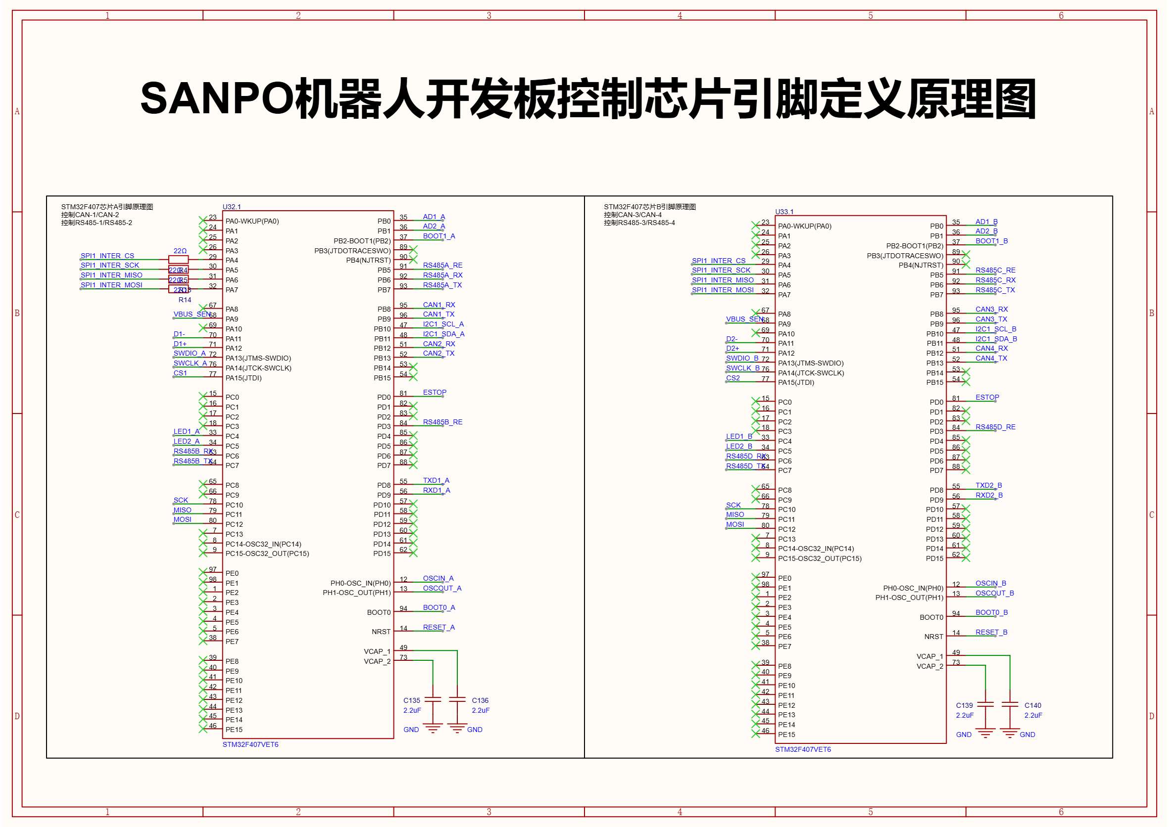
Interfaces Controlled by Each STM32
MCU |
CAN interfaces |
RS485 interfaces |
External SPI chip select |
USB and SWD |
|---|---|---|---|---|
STM32F407 (1) |
CAN-1, CAN-2 |
RS485-1, RS485-2 |
CS1 |
USB-1, SWD-1 |
STM32F407 (2) |
CAN-3, CAN-4 |
RS485-3, RS485-4 |
CS2 |
USB-2, SWD-2 |
When both MCUs perform the same function, program the same firmware through the two SWD connectors. Separate master and slave projects are needed only when the application uses the internal dual-MCU link.
Common Pin Assignment
The following table applies to both STM32 devices. “First channel” and “second channel” refer to the two interfaces managed by the current MCU.
Function |
STM32 pin |
Description |
|---|---|---|
ADC AD1 |
PB0 |
ADC1 IN8 |
ADC AD2 |
PB1 |
ADC2 IN9 |
Expansion UART TX |
PD8 |
USART3 TX |
Expansion UART RX |
PD9 |
USART3 RX |
I2C SCL |
PB10 |
I2C2 SCL |
I2C SDA |
PB11 |
I2C2 SDA |
External SPI CS |
PA15 |
SPI3 NSS; board connector CS1 or CS2 |
External SPI SCK |
PC10 |
SPI3 SCK |
External SPI MISO |
PC11 |
SPI3 MISO |
External SPI MOSI |
PC12 |
SPI3 MOSI |
First CAN RX |
PB8 |
CAN1 RX |
First CAN TX |
PB9 |
CAN1 TX |
Second CAN RX |
PB12 |
CAN2 RX |
Second CAN TX |
PB13 |
CAN2 TX |
First RS485 TX |
PB6 |
USART1 TX |
First RS485 RX |
PB7 |
USART1 RX |
First RS485 direction |
PB5 |
Transmit/receive switch |
Second RS485 TX |
PC6 |
USART6 TX |
Second RS485 RX |
PC7 |
USART6 RX |
Second RS485 direction |
PD3 |
Transmit/receive switch |
USB D- |
PA11 |
USB OTG FS DM |
USB D+ |
PA12 |
USB OTG FS DP |
SWDIO |
PA13 |
Programming and debugging |
SWCLK |
PA14 |
Programming and debugging |
LED1 |
PC4 |
Active low |
LED2 |
PC5 |
Active low |
ESTOP / reserved |
PD0 |
Reserved input |
RS485 TX and RX are listed by the STM32 peripheral function. Connect external devices to the board A/B terminals rather than to these logic-level pins.
Internal and External SPI
Pins PA4/PA5/PA6/PA7 of the two STM32 devices are already connected inside the board for dual-MCU communication:
Function |
STM32 pin |
|---|---|
Internal chip select |
PA4 |
Internal clock |
PA5 |
Internal MISO |
PA6 |
Internal MOSI |
PA7 |
No customer wiring is required for these signals, and they do not occupy the external CS1, CS2, SCK, MISO, or MOSI connectors. A Jetson, Raspberry Pi, or another host connects to external SPI3 on PA15/PC10/PC11/PC12.
Important Notes
Before wiring or programming, confirm which STM32 and interface group you are using.
The 3.3 V pin is an output. Do not apply external power to it.
Connect CAN and RS485 reference ground as required by the board version and device wiring diagram, and use suitable termination and communication settings.
Before changing the IOC or assigning pins, check this page and the schematic to avoid conflicts with USB, internal SPI, CAN, RS485, or SWD.